Basics
What is silicon photonics? The basics of the technology supporting optical communication
📌 Three-point summary
- Silicon photonics is a technology that uses semiconductor manufacturing processes (CMOS processes) to build optical circuits on a silicon substrate.
- Its adoption is spreading in a wide range of fields, including optical communication in data centers and LiDAR (a distance sensor that uses light).
- Material selection for the components that make up the outside of the chip (such as housings), not only the technology inside the chip, is also an important factor in the quality of the overall mounting.
What is silicon photonics?
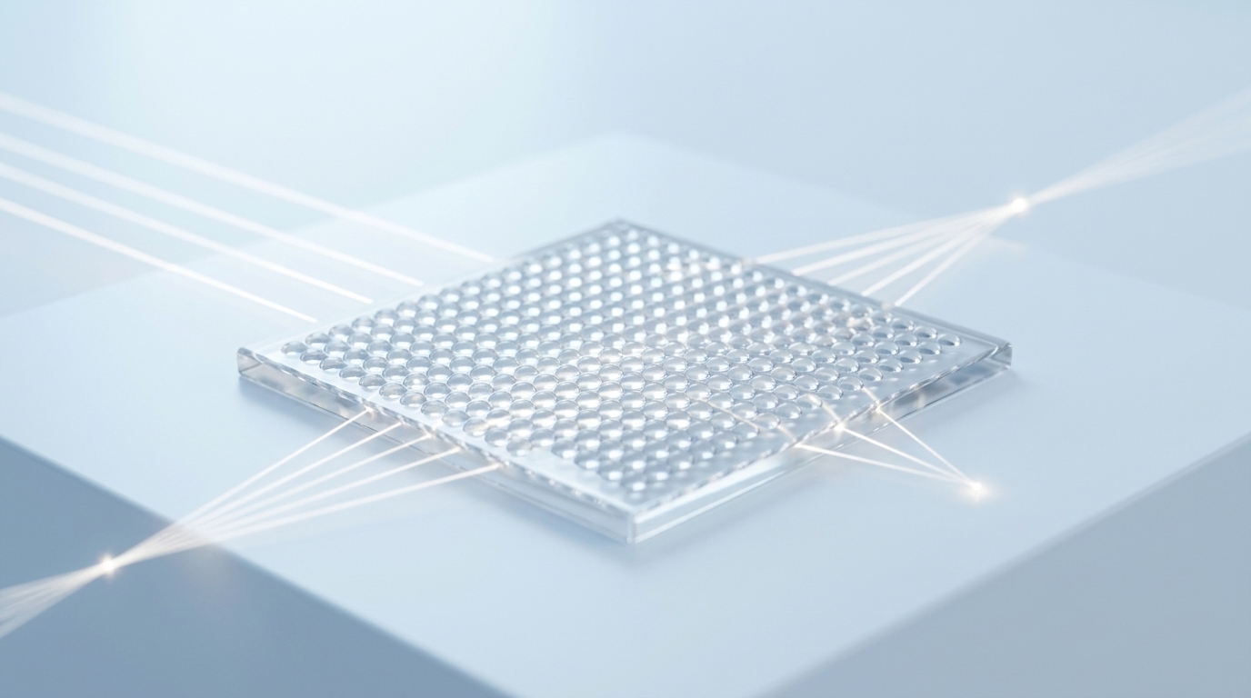
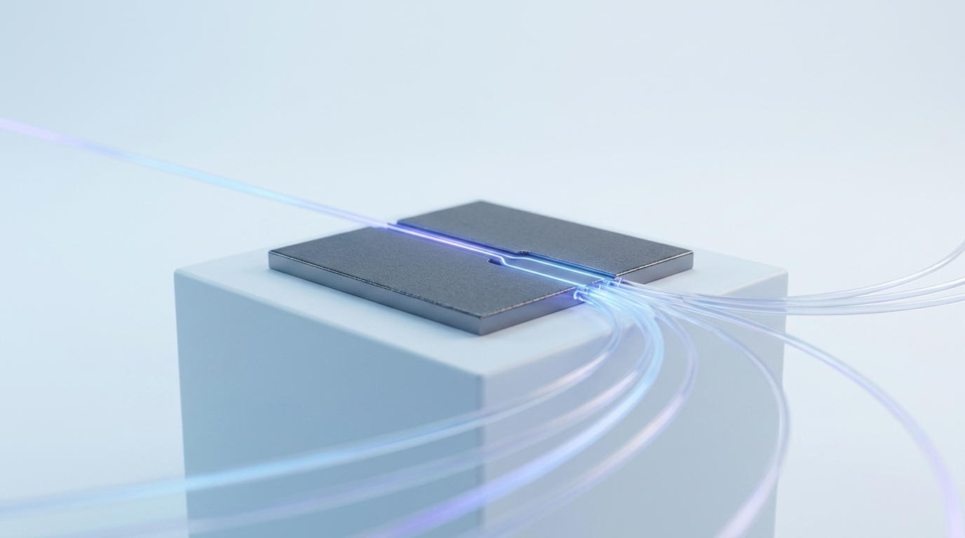
Silicon photonics is a technology that applies the CMOS process used to manufacture semiconductor chips (the standard manufacturing technology for making integrated circuits) to build circuits that guide light (optical waveguides) and components that convert light into electrical signals, integrated on a silicon substrate. Optical communication components have conventionally been made by combining separately manufactured optical parts, but silicon photonics can mass-produce optical circuits on the same manufacturing lines as electronic circuits, which makes miniaturization and integration easier.
This technology is attracting attention now because existing semiconductor manufacturing infrastructure (equipment and processes) can be repurposed. There is little need to create new materials or dedicated lines from scratch, which is said to be advantageous in terms of cost efficiency in mass production.
How it works: the principle of confining light in a waveguide
Light confinement through a refractive index difference
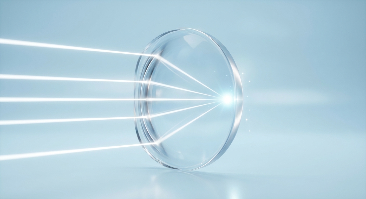
The core of silicon photonics is the “optical waveguide.” It is a structure that reproduces an optical fiber in miniature on a substrate, and it confines light to a fixed path by using the difference in refractive index (an index of how readily light bends) between the core, the part through which light passes, and the cladding, the part that surrounds it.
The refractive index of silicon (Si) is about 3.45 at a wavelength of 1.55 μm (1550 nm), while that of silicon dioxide (SiO₂, the main component of quartz glass), which is used for the cladding, is about 1.45. Because this difference is very large, light is reflected efficiently at the boundary between the core and the cladding, so that light can be confined and transmitted inside a thin waveguide.
Communication wavelength bands (1310 nm and 1550 nm bands)
Optical fiber communication uses specific wavelength bands called the 1310 nm and 1550 nm bands. These are widely known in the industry as “low-loss windows,” in which transmission loss (the degree to which light weakens) is low in silica-based optical fibers. The 1550 nm band has lower loss and is said to be advantageous for long-distance transmission, while the 1310 nm band tends to be used for medium-distance applications because its waveform spreading (dispersion) is small.
Main component devices and application fields
Basic configuration: light source, optical waveguide, modulator, and photodetector
A silicon photonics chip is broadly made up of the following elements:
- Optical waveguide: the path that carries the light itself
- Optical modulator: a component that converts electrical signals into changes in the intensity or phase of light
- Photodetector: a component that converts optical signals back into electrical signals
- Light source: a component that generates laser light (because silicon itself has low luminous efficiency, it is generally combined with another semiconductor material)
By integrating these on a single substrate, a circuit that converts between electrical and optical signals at high speed can be made compact.
Application fields
A representative application field is optical communication within and between data centers. In recent years, a mounting method called “co-packaged optics (CPO)” has attracted attention. This is a technology that places the semiconductor chip for switching (ASIC) and the optical engine that handles optical signals close together on the same package substrate, with the aim of easing constraints on power consumption and bandwidth by shortening electrical wiring. Applications are also expected in LiDAR (a distance sensor that uses light) used in autonomous vehicles and in the next-generation photonics-electronics convergence network infrastructure being researched in Japan.
Mounting challenges: not everything is solved inside the chip
Coupling efficiency and alignment accuracy as technical hurdles
For silicon photonics to be put to practical use, there is a challenge not only in the technology inside the chip but also in how to connect the chip and optical fibers with high precision. In particular, the “coupling efficiency” when connecting an optical fiber to a waveguide on the chip (how little loss there is when light is passed) and the alignment accuracy have been pointed out as mounting hurdles in several technical explainer articles.
Looking also at the components that support the outside of the chip
What handles this coupling and positioning are components that make up the outside of the chip: the FAU (fiber array unit, a component that arranges and holds optical fibers with high precision), which bundles and fixes fibers; the housing that protects the optical engine; and the holder for the microlens array (an optical component in which tiny lenses are arranged on a surface), which fixes lenses with high precision.
At present, materials such as quartz glass and ceramics are mainly used for these. Most technical explainer articles on silicon photonics focus on the circuit technology inside the chip, and few articles take the viewpoint of what materials these peripheral components are actually made of. However, when considering mass-production cost and weight reduction, material selection for the components outside the chip is also a point that cannot be ignored. In particular, as methods such as CPO, which mount optical engines at high density, spread, situations in which these components are also required to be smaller, lighter, and suited to mass production are expected to increase.
Iupizeta EP as an option
In the field of optical resins, the balance between refractive index (nd) and heat resistance (glass transition temperature, Tg) is important. As part of proposing materials suited to each application, Mitsubishi Gas Chemical is investigating development materials with higher heat resistance for its optical resin “Iupizeta EP.”
For example, Mitsubishi Gas Chemical is developing resins with the following properties.
Development material A: refractive index nd = 1.61, Tg = 264°C
Development material B: refractive index nd = 1.63, Tg = 280°C
Both show high internal transmittance in the 1310 nm and 1550 nm bands widely used in optical communication, and they are designed to secure the basic performance of an optical member while also meeting the heat resistance requirements that tend to be a challenge in the mounting process.
Furthermore, compared with thermoplastic polyimide (TPI) and polyetherimide (PEI), these development materials show markedly smaller dimensional change due to water absorption, which makes positioning accuracy and coupling stability easier to secure even under environmental fluctuation. Their birefringence is also far lower than that of TPI and PEI, making them suitable for applications that need to suppress polarization-dependent variation and optical distortion.
Anticipated applications include lens holding components, fixing and integrated components for optical members, and resin components around housings, that is, areas in silicon photonics mounting where optical properties, mounting heat resistance, and environmental stability must be satisfied at the same time. For details on applicability and conditions for specific required specifications, please feel free to reach out.
Summary: material selection in the age of silicon photonics
As high-density mounting methods such as CPO spread, the overall quality of mounting becomes visible when silicon photonics is considered not only as the optical circuit technology inside the chip but also with material selection for the packaging components that support it included. Optical resins such as Iupizeta EP are considered to be one of the options.
For details on Iupizeta EP, please reach out through the Iupizeta EP official website.
Some images and text in this article were created with the help of generative AI.


Recommended articles