Basics
What is a microlens array? How it works, applications, and manufacturing methods explained
📌 Three-point summary
- A microlens array is an optical element in which many tiny lenses, from a few μm to a few mm in size, are arranged on a flat surface
- Several manufacturing methods exist, including photolithography and precision glass machining, and microlens arrays are used in a wide range of fields such as optical fiber coupling, image sensors, and displays
- Microlens arrays are made of glass or resin, and the material must be selected to suit the application (a detailed comparison is given in a separate article)
What is a microlens array?
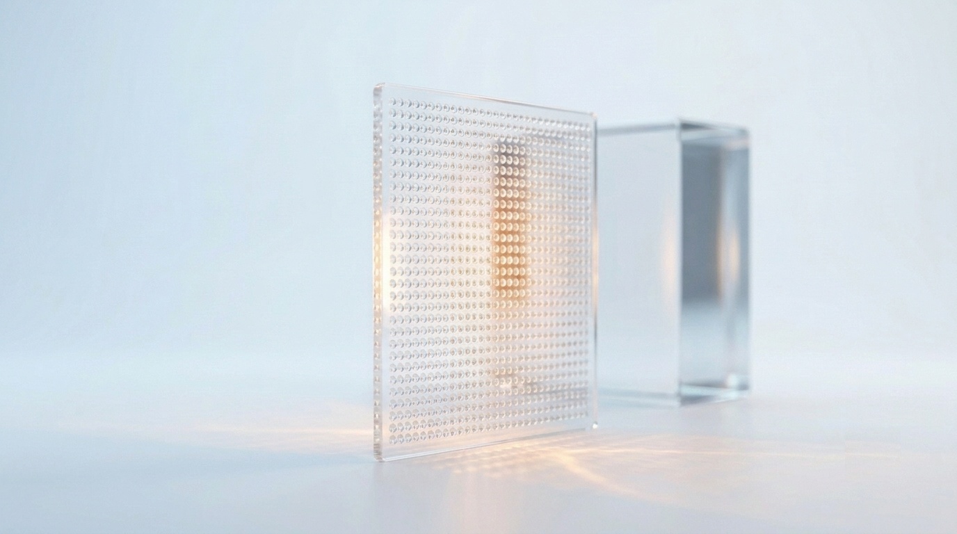
A microlens array (MLA) is an optical element in which many tiny lenses, from a few μm to a few mm in diameter, are arranged on a flat surface in a regular or irregular pattern. Because it looks like single lenses lined up in rows and columns, it is also called a “fly’s-eye lens.”
Each lens has the following functions, just like an ordinary single lens:
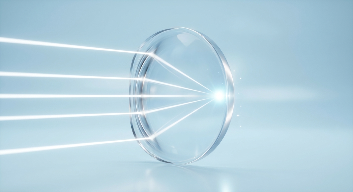
- Focusing: gathers light to a single point
- Diffusion: spreads light uniformly over a wide area
- Collimation (making light parallel): shapes diverging light into parallel rays
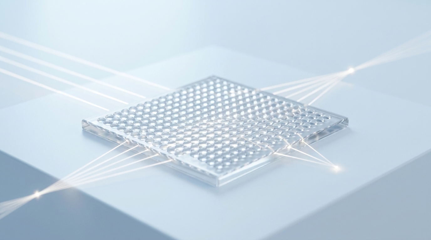
By arranging many of these small lenses over a surface, a microlens array makes possible “uniform light control” and “simultaneous focusing onto multiple points,” which are difficult to achieve with a single large lens.
Microlens array manufacturing methods
Microlens arrays are manufactured by several methods, depending on the material (glass or resin) and the required precision.
Photolithography and thermal reflow
This is a typical method widely used for resin microlens arrays. A photoresist (photosensitive resin) is exposed and developed to form cylindrical patterns, and then heated above the glass transition temperature (Tg) of the resist (heating at around 160°C has been reported). Surface tension causes the resist to deform naturally into a spherical shape, which gives a spherical lens form.
Mold transfer by electroforming and mass production
A master made by photolithography cannot be used for mass production as it is, so its pattern is transferred to a metal mold by electroforming (electroplating). Injection molding, compression molding, or hot embossing with this mold makes it possible to replicate resin microlens arrays in large quantities. Some resin injection molders also adopt a method in which the mold is machined by ultra-precision cutting and the arrays are produced by resin injection molding.
Imprinting and etching, and ultra-precision cutting and polishing of glass
Another approach is to form higher-precision patterns directly by imprinting or etching, which are microfabrication techniques close to semiconductor processes. Glass microlens arrays, on the other hand, are made by ultra-precision machining that cuts and polishes the glass directly, or by glass molding. That the suitable manufacturing method differs by material is a characteristic of microlens array manufacturing.
Main applications of microlens arrays
Microlens arrays are used in a wide range of fields that require precise control of light.
Optical fiber coupling
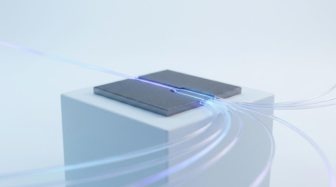
In optical communication equipment such as light source-to-fiber coupling, optical switches, and wavelength selective switches (WSS), microlens arrays raise coupling efficiency through collimation and focusing. For example, in NASA’s satellite observation project (the Ocean Color Instrument of the PACE mission), a target efficiency of 95% has been reported for coupling short-wave infrared light into a multimode fiber bundle. This is a target value for a specific project, and the coupling efficiency required differs depending on the application.
CMOS image sensors
In CMOS image sensors installed in digital cameras and smartphones, a tiny microlens is placed above each pixel to raise the efficiency of focusing light onto the photodiode. In backside-illuminated (BSI) sensors in particular, light-receiving sensitivity has been reported to improve by about a factor of two compared with frontside-illuminated sensors.
Displays, lighting diffusers, LiDAR, and sensing
Microlens arrays are also used as diffusers that spread light uniformly to achieve even illumination and wide viewing angles in displays. In LiDAR (a laser-based distance measurement and sensing technology), they are used for beam shaping and for improving light-receiving efficiency.
Use in astronomical instruments
Microlens arrays also have a track record in astronomical observation, a field that demands high precision. They are used in the Shack-Hartmann wavefront sensor mounted on the Subaru Telescope, which observes atmospheric turbulence in real time.
Material selection basics: glass and resin
Microlens arrays can be made from either glass or resin, and each has its own characteristics.
Glass microlens arrays have high heat resistance and environmental resistance, and low birefringence, the phenomenon in which light shows a different refractive index depending on its direction of incidence. However, grades that require high precision and low birefringence tend to incur higher costs for ultra-precision cutting and polishing and for dedicated mold machining.
Resin microlens arrays are characterized by excellent mass producibility, because they can be replicated in one batch from a mold by injection molding. On the other hand, they may require attention in terms of heat resistance and birefringence compared with glass.
Because the precision, operating environment, and production scale required differ by application, it cannot be said unconditionally which material is suitable. The reasons glass is regarded as the mainstream choice for optical fiber applications, and the problems that switching to resin can solve, are explained in detail with numerical data in our companion article.
Summary: avoiding mistakes in microlens array material selection
Microlens arrays are optical elements made by several manufacturing methods, from resin molding by photolithography to ultra-precision machining of glass, and they are used in a wide range of fields, from optical fiber coupling to image sensors, display diffusers, LiDAR, and astronomical observation. In material selection, it is important to understand the characteristics of glass and resin and to decide according to the application.
For help with optical resin selection, please reach out to Mitsubishi Gas Chemical through the link below.
Some images and text in this article were created with the help of generative AI.


Recommended articles